Description
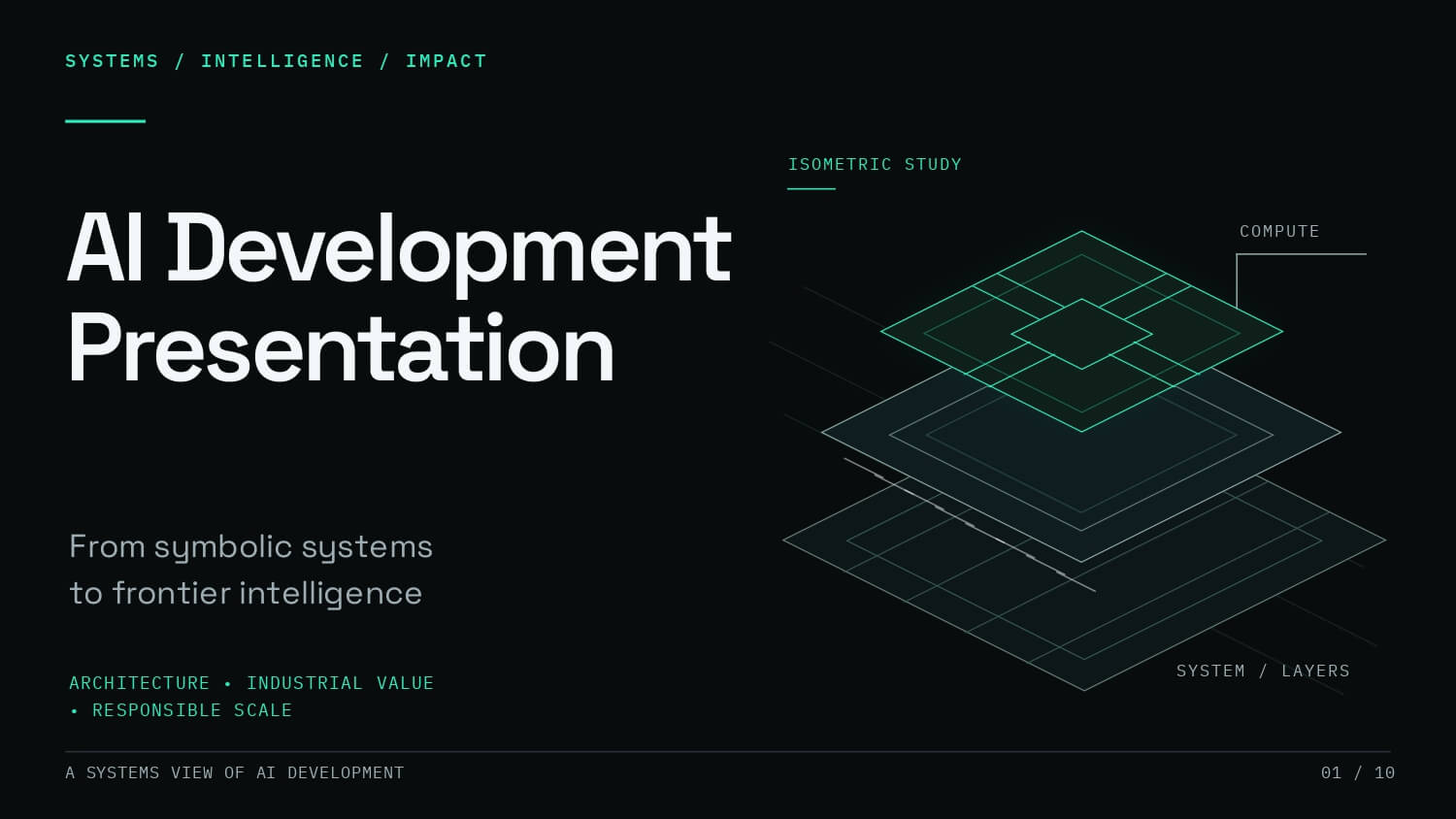
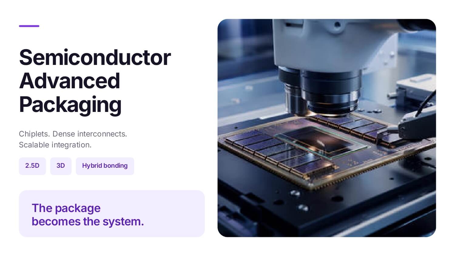
This semiconductor advanced packaging presentation template empowers chip founders and hardware engineers to pitch microelectronics innovations. The elegant deck features monolithic versus chiplet scaling shifts, 2.5D/3D packaging anatomy, wafer assembly process flows, and warpage-thermal yield matrices.
Main Features
- 16:9 aspect ratio
- 100% Fully editable elements
- Clean modern palette
- 3D architectural cutaways
- No design skills required
Create a presentation with this template
Describe your ideas and let HIX AI turn them into complete slides.